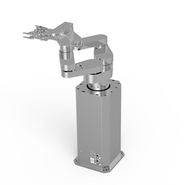
Imagine a factory cleaner than an operating room, where a speck of dust is catastrophic and a fingerprint spells disaster. In these hypersensitive environments, Semiconductor Wafer Handling Robots perform a ballet of precision, moving trillion-dollar silicon dreams across fabrication lines with superhuman accuracy. These aren't your typical factory arms; they are ultra-sophisticated machines enabling the AI chips powering everything from your smartphone to autonomous vehicles. Forget what you know about industrial robots – this is precision engineering pushed to atomic-scale limits.
Why Human Hands Are Banned: The Fragile World of Silicon Wafers
Semiconductor wafers, thin discs of ultra-pure silicon, are incredibly fragile and susceptible to contamination. A single human fingerprint can introduce enough oils or particles to ruin an entire batch, costing tens of thousands of dollars. Semiconductor Wafer Handling Robots operate within Class 1 cleanrooms (where fewer than 100 particles larger than 0.1 microns exist per cubic meter of air), eliminating the risks associated with human operators. Their movement precision, often measured in micrometers, ensures wafers are transported, lifted, placed, and processed without physical contact or the slightest vibration-induced defect.
The Robotic Nervous System: AMHS Explained
The true power of Semiconductor Wafer Handling Robots lies within the Automated Material Handling System (AMHS). This integrated network acts as the fab's central nervous system:
Overhead Hoist Transport (OHT): Robotic shuttles moving wafer pods (FOUPs/FOSBs) on ceiling-mounted rails between tool bays.
Equipment Front End Module (EFEM): The robot housed directly at the processing tool, loading/unloading individual wafers from the pod into the tool.
Automated Guided Vehicles (AGVs) / Rail Guided Vehicles (RGVs): Transporting materials between larger fab sections.
Modern AMHS relies heavily on AI algorithms, similar to those used in smart logistics seen in advanced Material Handling Robots, for dynamic scheduling, collision avoidance, and predictive traffic optimization, ensuring maximum throughput.
Vacuum vs. Atmospheric Robots: Masters of Different Domains
Not all wafer handling occurs in the same environment. Two primary robot types dominate:
Atmospheric Semiconductor Wafer Handling Robots
Operating inside the EFEM under standard cleanroom conditions, these multi-axis robots (SCARA or 6-axis designs) are blindingly fast, achieving wafer swaps in under 2 seconds. Key features include:
Ultra-low particle generation coatings and materials.
Precision vision systems for wafer alignment (notch finding).
Gentle, adaptive force control during wafer pickup/placement.
Vacuum Semiconductor Wafer Handling Robots
These specialized robots operate inside process chambers where atmospheric pressure is absent. Built for extreme environments:
Materials resistant to corrosive gases and high temperatures.
Magnetic or specialized drive systems eliminating lubricants (which could outgas).
Exceptional reliability – a single robot failure can shut down multi-million dollar tools.
The AI Connection: How Wafer Robots Feed the AI Loop
Semiconductor Wafer Handling Robots aren't just moving wafers; they are critical data generators feeding the AI systems optimizing modern fabs (also known as "smart fabs"). Every pick, place, move, and alignment generates telemetry data. AI systems analyze this real-time data to:
Predict Maintenance: Identifying subtle changes in motor vibration or alignment drift before failure.
Optimize Throughput: AI dynamically schedules robot movements based on tool availability and process bottlenecks.
Improve Yield: Correlating handling parameters (like placement force or orientation speed) with microscopic defects later discovered during inspection.
This integration exemplifies how automation and AI, explored further in our article on the Handling Robots revolution, are inextricably linked in advancing semiconductor manufacturing.
Beyond Silicon: The Expanding Horizons of Wafer-Scale Automation
While silicon remains king, the technology honed by Semiconductor Wafer Handling Robots is enabling breakthroughs in other demanding fields:
Photonics & Compound Semiconductors: Handling delicate GaAs, InP, or GaN wafers used in LEDs, laser diodes, and power electronics.
Advanced Packaging: Enabling heterogenous integration (chiplets) by precisely handling and aligning ultra-thin wafers and dies.
Quantum Computing: Transferring sensitive qubit substrates that demand extreme isolation from vibration and thermal fluctuation.
The Future: Angstroms, AI Synergy, and Extreme Mobility
As chip features shrink below 2nm and into the Angstrom era (?), the demands on Semiconductor Wafer Handling Robots intensify:
Atomic-Level Vibration Control: Robots will require active vibration cancellation systems integrated directly into their baseframes.
AI-Directed Precision: Real-time adaptive path planning using in-tool sensor data (temperature, gas flow) to compensate for nanometer-level distortions.
Hyper-Compact Designs: Smaller footprints needed for tighter integration within complex multi-process tools.
Enhanced "Sense of Touch": Advanced force-sensing end-effectors capable of detecting wafer flexures measured in nanometers.
Frequently Asked Questions (FAQs)
Q: Why can't standard industrial robots handle semiconductor wafers?
A: Standard robots generate excessive particles and vibration, lack the required micron-level precision for fragile wafers, and cannot operate effectively in the ultra-clean environments or vacuum chambers found in fabs. Semiconductor Wafer Handling Robots are built from the ground up for these extreme conditions.
Q: How do these robots prevent contamination?
A: They employ a multi-pronged approach: using special low-outgassing materials (e.g., specific ceramics, coatings), sophisticated filters on moving parts, hermetically sealed joints, minimizing sliding surfaces, rigorous cleaning protocols, and operating within HEPA-filtered environments. Particle counts are constantly monitored.
Q: What happens if a Semiconductor Wafer Handling Robot drops a wafer?
A: While extremely rare due to redundant safety systems, a dropped wafer is a catastrophic event, potentially representing a loss of tens of thousands of dollars and weeks of fabrication time. Fabs implement multiple safeguards – including vision verification, dual-arm coordination, and sensors confirming wafer presence on the end-effector at every stage.
Q: Are Semiconductor Wafer Handling Robots replacing all human jobs in fabs?
A: While automation handles the vast majority of physical wafer movement, humans remain essential for maintenance, programming, overseeing operations, engineering process improvements, troubleshooting complex tool issues, and performing R&D on next-generation processes. The role is shifting towards higher-level supervision and technical expertise.