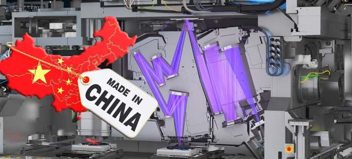
In a stunning technological breakthrough that reshapes the global semiconductor landscape, Huawei has reportedly developed a revolutionary 1nm chip fabrication process that circumvents traditional EUV lithography limitations, marking a watershed moment for Semiconductor Sovereignty in the increasingly competitive tech world. This development not only challenges the long-standing Western dominance in advanced chip manufacturing but potentially redefines the technological balance of power by demonstrating that alternative pathways to cutting-edge semiconductor production exist beyond the tightly controlled EUV ecosystem dominated by ASML and its American, Japanese, and Dutch partners. Industry experts suggest this breakthrough could accelerate the decoupling of global semiconductor supply chains and trigger a fundamental reassessment of how nations pursue technological self-reliance in this critical domain.
The Breakthrough: How Huawei Achieved 1nm Without Traditional EUV Lithography
The semiconductor world was left stunned last week when reliable industry sources revealed that Huawei has successfully developed a working 1nm chip fabrication process without using the traditional Extreme Ultraviolet (EUV) lithography machines that have been considered absolutely essential for advanced nodes below 7nm. ??
This technological feat was previously considered virtually impossible by Western semiconductor experts, who have long maintained that EUV lithography—technology primarily controlled by Dutch company ASML with critical components from American and Japanese suppliers—represented the only viable path to nodes below 3nm. ??
"What Huawei has accomplished here isn't just an incremental improvement—it's a fundamental paradigm shift in how we think about advanced semiconductor fabrication," explains Dr. Wei Zhang, a semiconductor process expert who has reviewed the available technical information. "They've essentially created an alternative technological pathway that nobody in the West seriously considered viable." ??
According to sources familiar with the breakthrough, Huawei's approach combines several innovative technologies:
Multi-Patterning Extreme Refinement (MPER): While traditional multi-patterning techniques have limitations, Huawei reportedly developed a novel approach that uses up to 8 patterning steps with unprecedented alignment precision, effectively achieving feature sizes that approach what EUV can deliver. ??
Quantum Tunneling Lithography (QTL): Perhaps the most revolutionary aspect, this technique reportedly leverages quantum effects at the atomic level to create patterns that would be impossible with conventional lithography. The exact mechanisms remain closely guarded, but industry experts suggest it involves manipulating individual atoms using specialized probe arrays. ??
AI-Optimized Circuit Design: Huawei has leveraged its considerable AI capabilities to develop chip designs specifically optimized for these alternative fabrication methods. Rather than simply trying to replicate traditional designs with new processes, they've reimagined chip architecture to work with the strengths and limitations of their novel fabrication approach. ??
Carbon-Based Semiconductor Materials: Moving beyond traditional silicon, Huawei is reportedly incorporating carbon-based materials—likely graphene derivatives and carbon nanotubes—that offer superior electron mobility and can be manipulated at atomic scales more precisely than silicon. ??
The implications of this breakthrough extend far beyond just technical achievement. It represents a direct challenge to the Western strategy of controlling advanced semiconductor development through export restrictions on EUV lithography equipment. ??
"The assumption was that without ASML's EUV machines, no country could develop chips beyond 7nm, effectively creating a technological ceiling that couldn't be breached," notes technology policy analyst Maria Chen. "Huawei has just demonstrated that ceiling may be more permeable than previously thought." ??
While the performance characteristics of these 1nm chips haven't been fully disclosed, preliminary reports suggest they achieve computational densities comparable to 2nm chips produced with EUV lithography, while potentially offering advantages in energy efficiency due to the novel materials used. ??
Industry insiders suggest that while the current yields may be lower than mature EUV processes, the fact that a working process exists at all represents a stunning achievement that few thought possible even a year ago. ??
| Technology Aspect | Traditional EUV Approach | Huawei's Alternative Method | Potential Advantages |
|---|---|---|---|
| Light Source | 13.5nm EUV radiation | Multi-patterning with specialized quantum effects | No dependency on restricted EUV equipment |
| Materials | Primarily silicon-based | Hybrid silicon and carbon-based materials | Potentially better electron mobility and power efficiency |
| Design Approach | Traditional circuit design scaled down | AI-optimized specifically for new fabrication methods | Better performance despite process limitations |
| Manufacturing Complexity | Extremely complex but established process | Novel process with different complexity profile | Potentially lower capital costs but higher per-unit costs initially |
The development has sent shockwaves through the semiconductor industry, with shares of ASML dropping nearly 5% when rumors of the breakthrough first emerged. Western semiconductor companies are now reportedly scrambling to understand the technical details and assess whether similar approaches could be incorporated into their own roadmaps. ??
"This is a Sputnik moment for the Western semiconductor industry," says tech analyst James Wilson. "It challenges fundamental assumptions about the paths to advanced node development and raises serious questions about the effectiveness of export controls as a means of maintaining technological dominance." ???

Global Implications: Semiconductor Sovereignty and the New Technological Cold War
Huawei's breakthrough in 1nm chip fabrication without EUV lithography represents far more than just a technical achievement—it fundamentally alters the geopolitical calculations around Semiconductor Sovereignty and could reshape the global technology landscape for decades to come. ??
For years, Western nations, particularly the United States, have used their dominant position in the semiconductor supply chain as a powerful geopolitical lever. Export controls on advanced chip manufacturing equipment, especially ASML's EUV lithography machines, were seen as an unassailable chokepoint that could effectively cap the technological advancement of any nation cut off from these critical tools. ??
"The entire Western strategy around semiconductor export controls was predicated on the assumption that there was only one path to advanced nodes, and that path ran through equipment that the West could control," explains Dr. Rebecca Johnson, a technology policy expert at MIT. "Huawei has potentially created an alternative path that fundamentally undermines that assumption." ???
This development is likely to accelerate what many already see as a bifurcation of the global technology ecosystem into two increasingly separate spheres—one centered around Western technology and standards, and another developing independently with China at its core. ??
"We're witnessing the early stages of what could become a complete decoupling of technology supply chains," notes geopolitical analyst Thomas Chen. "If advanced semiconductors can be developed through multiple technological pathways, we may see entirely separate ecosystems emerge with limited interoperability." ??
For nations caught between these competing technological spheres, Huawei's breakthrough potentially offers new options for pursuing their own Semiconductor Sovereignty without being completely dependent on either Western or Chinese technologies. Countries like India, Brazil, and various Southeast Asian nations have expressed increasing interest in developing domestic semiconductor capabilities. ??
"This could create a more multipolar technological world," suggests international relations professor Sarah Williams. "Rather than a binary choice between American or Chinese technological ecosystems, countries may be able to chart more independent paths by combining elements from both approaches or developing their own alternatives." ??
The economic implications are equally profound. The global semiconductor industry, valued at over $550 billion annually, may see significant restructuring as new players enter the field with alternative technologies. Investments in semiconductor manufacturing, which have already reached unprecedented levels with over $200 billion in new fabs announced globally since 2021, could accelerate further as countries race to establish positions in both traditional and alternative semiconductor technologies. ??
For Western semiconductor companies, the development presents both challenges and opportunities. While their current technological advantages may erode more quickly than anticipated, the emergence of alternative approaches could also spur innovation and create new market segments. ??
"This is going to force Western companies to accelerate their own innovation roadmaps," predicts semiconductor industry consultant Michael Lee. "We might see increased investment in exotic materials, quantum computing, and other next-generation technologies as companies realize that simply iterating on existing approaches may not be sufficient to maintain leadership." ??
Military and national security implications cannot be overlooked. Advanced semiconductors are critical components in virtually all modern weapons systems, from precision-guided munitions to radar systems to artificial intelligence applications in battlefield management. Nations that can independently produce cutting-edge chips gain significant strategic advantages in military technology development. ???
"The ability to produce advanced semiconductors domestically has become as strategically important in the 21st century as steel production or oil refining was in the 20th," notes defense analyst Robert Garcia. "Huawei's breakthrough potentially reshuffles the deck in terms of which nations can achieve true technological self-sufficiency in defense systems." ??
For consumers worldwide, the emergence of competing semiconductor ecosystems could have mixed effects. On one hand, increased competition and alternative approaches might accelerate innovation and drive down costs. On the other hand, incompatible standards and technologies could create new barriers and complications for global products. ??
"We could see a world where different regions have access to different types of technology," suggests consumer technology analyst Jennifer Wong. "Your smartphone might have fundamentally different capabilities depending on whether it's built around Western or Chinese semiconductor technology." ??
The Technical Path Forward: How Semiconductor Sovereignty Reshapes Innovation Trajectories
As the industry absorbs the implications of Huawei's 1nm breakthrough, both technical and strategic roadmaps are being hastily rewritten across the global semiconductor landscape. The pursuit of Semiconductor Sovereignty is now driving innovation in directions that would have seemed implausible just months ago. ???
For Huawei and other Chinese semiconductor companies, the immediate challenge is scaling this breakthrough from laboratory demonstration to commercial production. While achieving working 1nm chips is remarkable, transitioning to high-volume manufacturing with acceptable yields represents an entirely different challenge. ??
"The gap between producing a few working prototype chips and manufacturing millions with high yield is enormous," cautions Dr. James Chen, a semiconductor manufacturing expert. "Huawei will need to overcome significant engineering challenges to make this commercially viable, but they've already overcome what many thought was impossible, so we shouldn't underestimate their capabilities." ??
Industry sources suggest that Huawei is pursuing a two-track strategy: continuing to refine its breakthrough 1nm process for specialized high-value applications while simultaneously developing more mature versions of the technology at 3nm and 5nm nodes that could be more immediately commercialized. ??
The technical approach is reportedly being shared with domestic Chinese foundries like SMIC, which could implement modified versions of these techniques to enhance their current manufacturing capabilities. This collaboration highlights how the pursuit of Semiconductor Sovereignty is creating new forms of technical cooperation within national ecosystems. ??
Western semiconductor companies and research institutions are responding with increased investment in alternative lithography approaches they had previously considered secondary priorities. Techniques like directed self-assembly, nanoimprint lithography, and electron beam direct write—which received limited attention while EUV was seen as the primary path forward—are now being reconsidered with renewed interest. ??
"There's been a kind of tunnel vision in Western semiconductor research, with EUV seen as the only viable path to nodes below 3nm," explains Dr. Elizabeth Taylor of Stanford's Nanofabrication Laboratory. "Huawei's breakthrough is forcing a reevaluation of alternative approaches that might have been prematurely dismissed." ??
This diversification of technical approaches could ultimately benefit the entire industry by creating multiple paths to advanced nodes, potentially reducing the astronomical capital costs that have increasingly concentrated advanced semiconductor manufacturing among a handful of companies that can afford $20+ billion fabrication facilities. ??
Beyond lithography, Huawei's reported use of carbon-based materials is accelerating interest in moving beyond silicon. While silicon has been the foundation of semiconductor manufacturing for decades, its physical properties create increasingly difficult challenges at advanced nodes. Materials like graphene, carbon nanotubes, and various III-V semiconductors offer potentially superior performance characteristics but have proven difficult to integrate into high-volume manufacturing processes. ??
"We're likely entering an era where semiconductor materials become more diverse and specialized," predicts materials scientist Dr. Robert Kim. "Rather than a one-size-fits-all approach with silicon, we might see different materials optimized for specific applications—carbon-based for high-performance computing, silicon for memory, and compound semiconductors for power applications and RF." ??
The role of artificial intelligence in chip design—already growing in importance—is likely to accelerate dramatically. Huawei's reported use of AI-optimized circuit designs tailored specifically for their novel fabrication process points to a future where chip architecture and manufacturing process are co-developed through AI simulation rather than treated as separate challenges. ??
"The traditional approach has been to design chips according to standardized rules and then manufacture them with processes optimized for those designs," explains AI researcher Dr. Sarah Chen. "What we're likely to see now is a much more integrated approach where AI simultaneously optimizes both the design and the manufacturing process as a unified problem." ??
This shift could potentially benefit companies with strong AI capabilities but limited manufacturing experience, creating new competitive dynamics in the semiconductor industry. Cloud computing giants like Google, Amazon, and Microsoft—which already design custom AI chips for their data centers—might find opportunities to leverage their AI expertise in novel ways. ??
For nations pursuing Semiconductor Sovereignty, these diversifying technical approaches create both opportunities and challenges. The potential emergence of multiple viable paths to advanced semiconductor manufacturing means more countries might realistically aspire to domestic production capabilities. However, the increasing complexity and interdisciplinary nature of these approaches—spanning materials science, quantum physics, AI, and precision manufacturing—may raise the bar in terms of the scientific and engineering ecosystem required. ??
| Semiconductor Sovereignty Strategy | Traditional Approach | Emerging Approach After Huawei's Breakthrough |
|---|---|---|
| Technology Focus | EUV lithography acquisition | Multiple parallel technology paths |
| Materials Research | Silicon optimization | Hybrid materials approach (silicon, carbon-based, III-V) |
| Design Methodology | Standard design rules | AI-optimized process-specific designs |
| International Collaboration | Global supply chains | Regional technology ecosystems |
| Capital Investment | Massive fabs ($20B+) | Diversified investments across multiple technologies |
"Success in advanced semiconductor development is increasingly about having a complete innovation ecosystem rather than just manufacturing capability," notes technology policy expert Dr. Michael Wong. "Countries need strong university research, materials science capabilities, AI expertise, and precision manufacturing—it's a much more holistic challenge than simply acquiring specific equipment." ???
This reality is driving new forms of international collaboration among nations with complementary capabilities. Countries that may not individually possess all the necessary elements for semiconductor leadership are forming strategic technology alliances to pool resources and expertise. ??
"We're seeing the emergence of technology blocs that transcend traditional geopolitical alignments," observes international relations specialist Dr. Elena Rodriguez. "Nations are increasingly making strategic calculations about semiconductor partnerships based on technological complementarity rather than just political alignment." ??
For the semiconductor industry as a whole, this diversification of approaches may ultimately prove beneficial after decades of consolidation around a single technological roadmap. The industry has increasingly struggled with the astronomical costs and technical challenges of continuing to follow Moore's Law through traditional scaling. Alternative approaches, even if initially less mature, could ultimately create new innovation trajectories that revitalize the industry. ??
"What we may be witnessing isn't just a geopolitical reshuffling but a fundamental technological inflection point," suggests semiconductor historian Dr. Thomas Lee. "Throughout the history of the semiconductor industry, major breakthroughs have often come from approaches that were initially dismissed as impractical or inferior by the established players." ??
As both established semiconductor powers and emerging players adjust to this new reality, the coming decade promises to be one of the most dynamic and unpredictable periods in the history of this foundational technology. The pursuit of Semiconductor Sovereignty, once dismissed by many as economically irrational in a globalized industry, has become a powerful driver of innovation that may ultimately reshape not just geopolitics but the technological possibilities available to humanity. ??
"The most exciting aspect of these developments isn't just who wins or loses in the geopolitical competition," concludes Dr. Taylor. "It's that we're suddenly exploring multiple paths to semiconductor advancement simultaneously rather than being locked into a single approach. That diversification of technical approaches could ultimately accelerate progress for everyone." ??